Category Archives: Blog

Issue 23: Coming Soon, Non-transitive Clock Domains for CDC Analysis (and Why They Matter)

David E. Wallace – Chief Scientist, Blue Pearl Software

There is a new development in the Clock Domain Crossing community that will affect both developers and users of CDC tools. For the past year, a working group of interested companies has been developing a new draft standard for CDC collateral that should allow tools from different vendors to cooperate in verifying different pieces of a large design. This CDC Working Group, organized under the Accellera Systems Initiative, released the 0.1 version of the draft standard for public review and comment on October 31st. The 0.1 version of the draft standard is primarily focused on representing CDC information at module boundaries. Future versions of the draft standard are expected to additionally address Reset Domain Crossings and Glitch Analysis.

You can find out more information, including where to download the draft standard and submit comments at https://accellera.org/news/press-releases/385-accellera-clock-domain-crossing-draft-standard-0-1-now-available-for-public-review. Note that the public comment period for this version of the draft standard will end on December 31st, 2023.

Blue Pearl Software has been actively participating in this working group and in the Preliminary Working Group that preceded it. We consider it important that users of our CDC tool should be able to interact with portions of the design that may be analyzed by other tools, whether to incorporate IP blocks or to use the design we analyze as part of a larger design. We have also benefited from broader discussions about CDC from users who are not part of our customer base.

Today, I would like to discuss one aspect of the draft standard that will require some changes in the way we do our CDC analysis. The draft standard allows for the possibility that users may define which clocks are synchronous to each other in a way that requires Non-transitive Clock Domains to describe.

What are Non-transitive Clock Domains?

Up until now, we at Blue Pearl have viewed Clock Domains as a form of equivalence class, in which clocks within a given clock domain are all synchronous to each other and asynchronous to any clock in a different domain. This equivalence class implies three properties of the binary relationship known as “is synchronous to”: the relationship is reflexive (clockA is synchronous to clockA), symmetric (if clockA is synchronous to clockB, then clockB is synchronous to clockA), and transitive (if clockA is synchronous to clockB, and clockB is synchronous to clockC, then clockA is synchronous to clockC). If all three properties hold, then we can group the clocks into distinct clock domains, where every clock is a member of one and only one domain.

A Non-transitive Clock Domain, then, is a case where the third property need not hold: where clockA is synchronous to clockB, and clockB is synchronous to clockC, but clockA and clockC need not be synchronous to each other. The primary use case that was discussed in the working group where users wanted this capability involves two different derived clocks whose clock periods do not evenly divide each other.

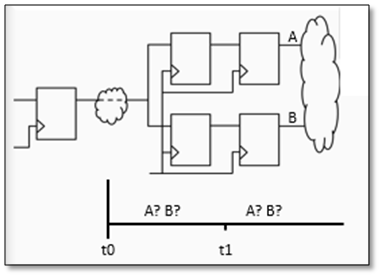
An example of this is shown in Figure 1 below. It involves a base clock in blue (“Base”) and two derived clocks, a divide by 3 clock in green (“÷3”) and a divide by 4 clock in orange (“÷4”). The rising edges of all three clocks are shown in the diagram to the right in terms of the number of cycles of the Base clock.

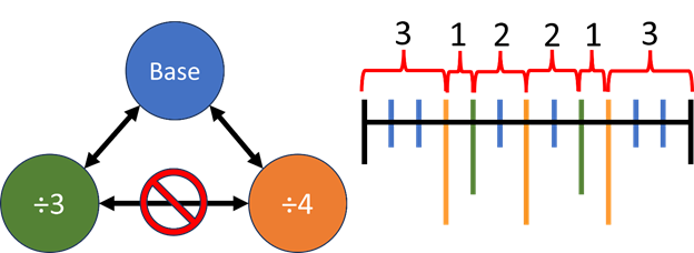
Figure 1: Base clock with two derived clocks that are treated as asynchronous to each other.

Now it is certainly possible to treat all three clocks as synchronous. They meet the definition we at Blue Pearl have used for synchronous clocks, in which two clocks are synchronous if the edges of both can be described using selection and translation of edges from a common ideal clock. However, there are reasons why a designer might choose to treat the two derived clocks as asynchronous instead.

To treat these clocks as synchronous and verify resulting paths in static timing analysis, the paths from registers clocked by ÷3 to registers clocked by ÷4 would need to be limited by the closest approach of two edges from those clocks, which would be a single cycle of Base (less any possible skew between the two). This is considerably shorter than the period of either of the two clocks involved. Moreover, because the two clock zones produce and consume data at different rates that are not clean multiples of each other, the user may want to use FIFOs on paths between the two to smooth out the flow of data. By treating the two clocks as asynchronous and using CDC analysis to verify that any paths between the two clocks are synchronized by FIFOs or other acceptable synchronizers, the user can verify that all data flowing between the two is properly synchronized.

To describe this kind of relationship, where “is synchronous to” is not necessarily transitive, the draft standard allows a clock to belong to more than one clock domain. Two clocks are considered synchronous if there is any domain that contains both clocks. Otherwise, they are considered asynchronous by default, and CDC analysis will check that any path between them is properly synchronized. The relationship between the clocks in Figure 1 can be described with two clock domains: domain1, which contains Base and ÷3, and domain2, which contains Base and ÷4. Thus, Base is considered synchronous to each of the two derived clocks, because it shares a domain with each, but the two derived clocks are considered asynchronous to each other because there is no single domain that contains both.

To represent these clock domains, the draft standard introduces a new command, set_cdc_clock_group. This command is similar to the SDC set_clock_groups command, however it defines a set of mutually synchronous clocks that constitute a single clock domain. Clocks are presumed asynchronous by default, unless they explicitly share a clock domain, which is the appropriate default for CDC analysis. (Technically, this draft of the standard is not defining a formal syntax for the command yet, but the syntax of a Tcl implementation is expected to look much like the pseudo-code in examples such as Figure 15 of the draft standard.)

What will this mean for our users? Users who are happy with conventional transitive clock domains should be able to continue to work much as they have been. To date, we have been using the SDC set_clock_groups command with nonstandard, more CDC-friendly semantics to define and save our clock domains. We intend to migrate to the new set_cdc_clock_group command as the primary way to represet clock domains going forward, while maintaining compatibility options for users who want to read SDC files with our old semantics.

For users who do have a need for non-transitive clock domains, they will soon be able to express those relationships in our tool using set_cdc_clock_group commands. There will likely be some new options that may help support this style of work. We are likely to release individual features as they become available, rather than waiting for one big release that incorporates the whole of the new draft standard. Indeed, the draft standard is very much a work in progress that will change in response to public feedback and continued work by the working group. We also want to hear from our users and potential users on what you consider the most important features for us to implement from this draft standard. Please let us know your questions and thoughts at V0-1Priorities@bluepearlsoftware.com.

Conclusion

It is our hope that adoption of this new interoperability standard will benefit our users by making CDC analysis more efficient and complete, regardless of which other tools are employed by our users or their IP vendors. We encourage you to read the proposed Accellera standard and give your input by December 31st using the links provided above. We also encourage interested companies to join Accellera and participate with us in the CDC Working Group to help define the next stages of the standard.

To learn more about the Visual Verification Suite please request a demonstration.

Issue 22: When debugging it’s always either the reset or the clock!

FPGA designs are becoming very complex for many FPGA developers. One thing that often causes issues during integration of IP and proprietary blocks is that of resets and clocks. In this blog we will look at resets and how they are used varies from device to device.

Starting with the basics, we use reset to drive all the registers within a design to a known state at power on or whenever it is commanded during normal operation. This ensures all registers are in a known state and operation of the device will be as expected and simulated. Reset therefore prevents FSMs from starting off in states mid-way through the flow due to the random power on register states.

However, not all FPGA technologies recommend the use of resets. For example, SRAM based FPGAs typically have a global set/reset which is applied as part of the configuration sequence. This has several benefits for the developer as it significantly reduces the number of control signals which are in the design, enabling a better quality of implementation. It also provides the implementation tool more choice in which resources are used, e.g. D vs SRL. Of course, not all of the design may be reset free in a SRAM based FPGA. However, typically the reset will be limited to the control path.

If, however, we are targeting a FLASH based or One Time Programmable FPGA or have hopes to migrate to an ASIC if volume is achieved then, a reset is definitely required for all of the registers in a device.

For all types of FPGAs, the debate will then become if the resets should be asynchronous or synchronous. This will depend upon the architecture of the device itself. You may also find that some element can only accept one reset type, for example DSP elements.

When it comes to creating FPGA code which is portable between all device technologies, something all engineers should be striving for to reduce non-recurring expense, ensuring the RTL can be configured either way via generics or parameters is of importance.

This can be achieved using constants, generics or parameters depending upon which language you use to develop your FPGA. An example VHDL implementation would appear as follows:

if set_asynch_rst and rst = set_rst_pol then
         q <= '0';         -- asynchronous reset configuration
elsif rising_edge(clk) then
         if not set_asynch_rst and rst = set_rst_pol then
                 q <= '0'; -- synchronous reset configuration
         else
                 q <= d ; -- functional operation
         end if;
end if;

This allows the developer to specify either no reset, asynchronous, or synchronous reset styles, along with the reset level. This give maximum flexibility to the developer as to which technology is targeted. With higher level tools like HLS we also get the ability to control the reset type.

However, with flexibility around this reset strategy comes the potential impact of getting it wrong, e.g., a misbehaving design from an un-reset register or failing timing from an unnecessary reset. It is important to be able to check all of the reset conditions:

  1. 1. Registers are reset
  2. 2. Registers are applied synchronous reset
  3. 3. Registers are applied asynchronous reset

Here is where Blue Pearl’s Visual Verification Suite can be of assistance, with its ability to analyse the reset structure and report on the reset configuration of the design as currently configured.

Blue Pearl Software’s Visual Verification Suite can report on a range of reset configurations combined with define scenarios of parameters / generics to ensure the reset structure is as required for the design.

The suite will also report on the reset level, providing peace of mind so that the design does not have mixed reset levels, which again would impact the design performance and lead to long debugging sessions.

Applying the right reset strategy for your design can increase performance and ensure your design is not going to behave incorrectly following power on. The Visual Verification Suite can aid you in verifying you have implemented the correct reset structure for your target design quickly and easily, enabling you to go into implementation with peace of mind, on this issue among others!

To learn more about the Visual Verification suite or to discuss how you can integrate it inside your revision control system, please request a demonstration.

Issue 21: Using Revision Control Systems with the Visual Verification Suite

Continuous Integration and Continuous Deployment (CI/CD) used in the development of FPGA, ASIC and Intellectual Property cores is a process of build automation and RTL code testing each time the development team makes changes under version control. The practice is focused on improving hardware quality throughout the development life cycle via automation.

During the CI/CD process, developers share and merge their changes (code and unit tests) into a version control repository. Adopting a continuous integration approach is one of the most beneficial and low-cost practices individuals as well as teams can implement in terms of improved quality and efficiency.

Some of the advantages of adopting CI/CD tools include:

  1. Continuous feedback – Fault isolation so that when an error occurs, the negative consequences are limited in scope
  2. Reduced friction – Prevention of merge conflicts such as bugs and duplicate code, making for cleaner code and fewer issues later in the design cycle
  3. Higher speed / faster release rate – Accelerated code reviews and decreased development time by automating time consuming tasks
  4. Lower cost with easier maintenance and updates – With a CI/CD approach, developers can make sure that the product is updated and maintained at frequent intervals

In the development of FPGA, ASIC and Intellectual Property cores, projects may involve multiple team members with distributed responsibilities, such as sub-module design, device and system integration, verification, and timing closure. In such cases, it is useful to track and protect file revisions in an external revision control system.

Jenkins is an open-source, free CI/CD server written in Java. It works with multiple programming languages and can run on various platforms (Windows, Linux, and macOS). As such, Jenkins is one of the most popular open-source tools on the market for automating projects. The Visual Verification Suite has been designed to work with any version control system such as Bamboo, Buddy, TeamCity, GitLab, Jenkins and others. However, for this example we will take a closer look at Jenkins integration.

To recreate an analysis run initiated using the GUI, Blue Pearl recommends that the following files, written by the Visual Verification Suite GUI into the Results directory, are stored in the revision control system along with the RTL project source files:

  • bluepearl.runme.tcl
  • Project_Name.settings.tcl
  • Project_Name.bluepearlgenerated.f

Then run, in command line mode:
>BluePearlCLI -f Project_Name.bluepearlgenerated.f

The Visual Verification Suite will restore the project using the settings stored in the Project_Name.settings.tcl file. Please note that the two files that start with Project_Name are generated with explicit path references that may need to be edited. Relative path references are allowed.

After the analysis has been run, the bluepearl.runme.tcl script has a call to “exit” the Tcl shell. Users can edit this out if they wish to continue interactively with analysis and debug after restoring the project.

The tool creates the following databases required for analysis in the Visual Verification Suite:

  • bluepearl.bpsvdb – the Blue Pearl visual data base
  • modinfo.db – the database for the design
  • results.db – the database with the static analysis results

In addition, because the suite can be configured to run different features, we recommend having different directories for different options. For example, if the Analysis is configured for Long Path Analysis only in the Project_Name. bluepearlgenerated.f file, modify the output directory to have the name: Results_LP. Likewise, for just a CDC run, rename the directory to be: Results_CDC.

In addition, the waivers.xml file is a database of sorts. It contains all the waivers and their timestamp/owner combinations. This file may be source code controlled because it can be manually and graphically edited, thus changing results reported by the tool. It is also possible to use multiple waivers files simultaneously, so that different groups or designers can keep separate waivers files that can be configured to work both on submodules and the entire design.

When running a revision control system like Jenkins, it is possible to set it up to automatically run the Visual Verification Suite as a mandatory step prior to making source RTL changes. This will prevent structural RTL errors from entering the Simulation scripts. Additionally, it is also possible to set up to run prior to simulation. If no new messages are found, then simulation is called.

Blue Pearl has worked with Jenkins to be supported in the Jenkins Next Generation Warnings plugin where the tool performs a textual analysis of the log file, summarizing the number of warnings and errors. In addition, the Visual Verification Suite ships a Jenkins plugin called “RunBluePearl” that is used to integrate any specific version of Jenkins.

The “RunBluePearl” plugin allows the BluePearlCLI to be added as a build step in a Jenkins flow. In addition to design setup, global settings include licenses and installation, while the tool is configured to report all errors and warnings (not just the usual limited number of messages), to allow textual analysis of the log file.

Incorporating a CI/CT tool in the development of FPGAs, ASICs and Intellectual Property cores is a must-have element of the development process. When choosing a tool, make sure to pick the one that best fits your project and business requirements, and don’t worry, the Visual Verification Suite is designed to work with it, speeding and simplifying the development and verification processes at the same time.

To learn more about the Visual Verification suite or to discuss how you can integrate it inside your revision control system, please request a demonstration.

Issue 20: Code Quality, It’s a Matter of Style

Code quality is essential to staying on schedule, avoiding design iterations and worse, bugs found in production. For any design team, creating readable and maintainable code that everyone understands takes some common discipline, starting with the basics such as naming conventions. It’s not so much whether the organization prefers big endian or little endian, spaces or tabs, prefixes or suffixes, underscores or hyphens or camel case, the important thing is to have a coding standard and stick to it. By standardizing on naming conventions for instances, modules, signals, clocks, resets, architectures, packages, and so on, code becomes clearer and reusable and, as a side benefit, it reduces the code complexity.

Blue Pearl Software’s Visual Verification Suite (VVS) includes a variety of naming checks that offer enormous flexibility and scope. Users specify parameters for each activated check using regular expressions.

Name Analysis vs. Identify

The tool includes two kinds of naming parameters and checks. First, there are parameters that pertain to rules about names assigned to objects and items of a known type. Since the tool has identified the object or item as being of a specific type, it can then check the name against the parameter to see if it is properly named. We label such checks and parameters as Name Analysis. There are numerous types of objects and items covered by Name Analysis parameters and checks, most having multiple sub-types. The bulk of this paper concerns these Name Analysis items.

Second, there are parameters intended to assist the tool in determining the object type, or to declare that objects of a given sort are not to be flagged. For example, in the case of a gated clock, it is often the designer’s intent that one input of the gate be the clock itself and the other be an enable. It might be necessary to assist the tool by declaring that a signal that conforms to a given naming parameter is an enable rather than a clock.

You may also have in your design nets that are tied to one or zero, or signals or pins that are intentionally left dangling. You will want to prevent the tool from flagging these as issues.

We label these sorts of checks and parameters as Identify. The objects that can be Identified are Clock Gating Signals, Reset and Set signals, Dangling signals and pins, Static Control Registers, and nets Tied high or low. Each of these has a corresponding IDENTIFY check and a corresponding parameter that can be set as described above. There are also two additional parameters that can aid the tool in identifying top level clocks and internal clocks.

Global, Object type, and Sub-type

The types of items whose names can be analyzed include: Filenames, Modules, Ports, Signals, Instances, Function Names, Labels, Constants, Language Keywords, Constant Value, Data Types, Port Data Types, Generic Data Types, Operator Parameter Names and Types Names, VHDL Others Assignments, Verilog Include Files, and Libraries. In addition, it is possible to specify Global naming rules that apply to all objects. For example, it is common to strictly forbid consecutive underscores throughout the design. One might also have a list of forbidden keywords.

With a few exceptions, each type has one or more sub-types, which in turn may have one or more sub-sub-types. For example, the three sub-types of Ports are Inputs, Outputs, and Inouts. Each of these has a sub-sub-type for buses, such as Input buses. Each of these is further sub-divided into Top Level and Sub Level.

For each type and at all levels of nesting, the user can specify a Regular Expression which the name of a particular item must match, and a Disallowed Regular Expression which the name must not match. Violations detected by Allowed and Disallowed expressions produce separate messages. In addition, the user can choose whether these expressions (allowed and disallowed) will apply to the full hierarchical path name, whether the expressions will be considered case-insensitive, and whether the specified expressions will be applied in lieu of, or in addition to, the expressions covering its parent type.

To specify any such parameters for a given type, the corresponding NAME_ANALYSIS check must be enabled. For example, you cannot specify a Regular Expression for Outputs if the NAME_ANALYSIS_PORTS check is not enabled. In some cases, a sub-type may have its own check. For example, under Signals each of the available sub-types (Registers, Clocks, Resets, Sets, and Clock Gating/Enabling Signals) is governed by its own check. This is in addition to the NAME_ANALYSIS_SIGNALS check and its corresponding parameter since there are signals which do not belong to any of the available sub-types.

Variables

There are several design-specific variables that can be used as part of the regular expressions. For example, you might use the ${FILE} variable to indicate that the base filename would be part of the regular expression. Some variables have restrictions are their use. For example, ${ENTITY} can only be used with VHDL, and ${PARENT_CLOCK} can only be used during clock analysis.

Conclusion

Having robust and specific naming rules can enhance the readability and reusability of your RTL code. The Visual Verification Suite provides regular expression-based naming rules that offer greater flexibility and scope than other methods.

Used early and often in the design process, as opposed to as an end of design/sign-off only tool, significantly contributes to design security, efficiency, and quality, while minimizing chances of field vulnerabilities and failures.

To learn more about the Visual Verification suite, please request a demonstration.

Guest Blog: Using Blue Pearl Software to Find Clock Domain Crossings

Adam Taylor CEng FIET• 1stEmbedded Systems Consultant, FPGA Expert, Prolific FPGA Writer

A few weeks ago, we talked about how we could synchronise between clock domains in Vivado, I also noticed a couple of questions on r/FPGA about tools which could be used to find CDCs in designs. So, I thought it might be a good idea to blog about how we find CDC at Adiuvo Engineering and Training.

Of course, most vendor tools provide the ability to find CDCs in your design however, as they are not specialised for CDC the reports which are presented and debugging views can be a difficult to interpret. So just as vendors supplied simulation tools are often not used professionally opting for a higher performance simulation tool instead, it is common to use a third-party CDC tool.

Within Adiuvo we use Blue Pearls Visual Verification Suite to ensure our designs have no CDC issues. This works well for us as several of our clients including the European Space Agency use Visual Verification Suite for CDC and structural analysis.

One of the benefits of using VVS is that the analysis is conducted on the actual RTL therefore there is no need to wait for synthesis to complete before the analysis can be used. The tool is also vendor independent so we can use it to verify RTL designs that we might want to reuse across several vendors.

Let’s look at how we can find a CDC using VVS. Blue Pearl works in two stages, the first stage is loading in the design during which the RTL is checked using the Verific parser for LRM compliance. The design is also check for completeness e.g., are all the source files present and we do not have any missing blocks which would become black boxes and prevent the correct CDC analysis.

Once the design is loaded successfully, we can run the more detailed analysis options, one of these is CDC, the others are path analysis – identifying longest paths in the design and Multipath and False path identification.

To be able to do CDC analysis we need to have informed the tool of which vendor we are using, VVS has built in vendor libraries which enables the CDC analysis to be formed on design including IP. VVS does this by creating what is known as grey cell for the IP being used the grey cell includes only the input and output rank of flip flops. Knowing the clock domains of the IO enables VVS to determine if a CDC has been introduced.

The CDC analysis itself takes only a few minutes to analysis the RTL and produce a list of potential CDC for the engineer to investigate.

Clicking on the failing CDC path will cross probe not only to the source code but draw a schematic diagram which shows the failing path.

In the example above it shows the insertion accidently of a CDC as the FIFO empty signal is associated with the read clock, but it has been used with the write clock without appropriate clock domain crossing protection.

We find the visual analysis of the potential CDC and the cross probing to the source code very useful; it enables us to quickly home in on the area of code which might be a problem.

The reports are also very useful when it comes to gaining acceptance and sign off from clients as part of the design assurance process, as we can demonstrate the CDC checks have been performed.

Issue 19: A slogan is just that, a slogan

A slogan is just that, a slogan or sometimes referred to as a tag line. Something catchy, something fresh and, of course, something we hope you don’t forget. So, with Blue Pearl Software’s slogan, ‘verify as you code’, we hope it conjures up a feeling that as you code, a smart editor is keeping watch. Making sure no mistakes sneak into the design, be it syntax, structural and even security issues.

So, what’s behind our slogan? Twenty-four years of technology to start with. Simply put, we have been helping HDL (VHDL / SystemVerilog) developers for quite some time. Over these years, we have refined the Visual Verification Suite to help FPGA and IP developers find critical issues up front in the design process, saving both time and money. We can honestly say, when you write code using the Visual Verification Suite’s HDL Creator smart editor, your HDL is verified as you code.

HDL Creator is ideal for developers coding both RTL and test benches who are seeking productivity, predictability and code quality for complex FPGAs and IP. HDL Creator provides real-time syntax and style code checking inside an intuitive, easy-to-use full featured editor. Unlike standard editors, HDL Creator provides advanced real-time file analysis to find and fix complex issues as you code, such as compilation dependencies and missing dependencies.

HDL Creator is a full-featured source code editor that provides all the normal features you would expect from a modern code editor such as autocomplete and error fix suggestions. HDL Creator provides over 2000 real time syntax and customer specific coding standard checks to streamline code development, saving time and effort all while averting common coding mistakes that could result in downstream design iterations. HDL Creator also provides advanced design views to help understand, verify, and debug as you code.

In addition to HDL Creator, the Visual Verification Suite also provides advanced static and formal RTL analysis to identify coding style and structural issues up front. While not real-time, like HDL Creator, the suite’s RTL Analysis points out 100’s of additional potential structural issues such as:

  • Unnecessary events – These are unnecessary signals included in the sensitivity list. Such inclusion will lead to simulation mismatch and add complexity to achieving code coverage.
  • If-Then-Else Depth – This will analyze the If-Then-Else structures to identify deep paths which may impact timing performance and throughput when implemented.
  • Terminal State – This is a state in a state machine which once entered has no exit condition. Finding this prior to simulation can save wasted simulation time.
  • Unreachable State – This is a state in a state machine which has no entrance condition. Finding this prior to simulation can again save considerable simulation time.
  • Reset – This ensures each flip flop is reset and reset removal is synchronous to the clock domain of the reset. Several in-orbit issues have been detected relying upon the power-on status of registers and as such reset for all flip flops is best practice.
  • Clocking – Clocking structures are also analyzed to ensure there is no clock gating or generation of internal clocks.
  • Safe Counters – Checks counters to ensure that terminal counts use greater than or equal to for up counters and less than or equal to for down counters. This ensures single event effects have a reduced impact on locking up counters.
  • Dead or unused code – Analyzes and warns about unused or dead code in the design. This can be removed prior to functional simulation and reduces head scratching when code coverage cannot be achieved.
  • Clock domain crossing – Ensuring clock domain crossing are synchronized to avoid metastability issues.


Figure 1: Visual Verification Suite’s CDC Viewer

So, what is it that makes the Visual Verification Suite such a powerful debugging environment? It runs on Windows or Linux, and lets you easily move back and forth between command line mode and a straightforward, understandable graphical user interface. It can quickly generate reports that show aspects of your design in general, like your highest fanout nets, or your longest if-then-else chains, and an easy-to-filter report window showing the specific issues it has found. The suite also includes numerous checks to catch violations of company specific naming conventions.


Figure 2: Finite State Machine Viewer

Design teams that leverage static verification as part of their functional verification methodology are proven to reduce hardware security risks, as well as expensive and time-consuming simulation, synthesis and place and route runs and reruns, freeing up expensive licenses as well as improving overall design productivity.


Find and fix issues as you code, not late in the design cycle

Blue Pearl’s Visual Verification Suite, used early and often in the design process as opposed to as an end of design/sign-off only tool, significantly contributes to design security, efficiency, and quality, while minimizing chances of field vulnerabilities and failures.

We hope our slogan, ‘verify as you code’ comes to mind the next time you or your team develops an FPGA. To learn more, we encourage you to sign up for a demonstration to learn more how the Visual Verification Suite can ensure quality code for high reliability FPGAs.

Issue 18: So, what’s a Grey Cell anyway…

They say with a chain, it is only as strong as its weakest link. The same can be said about an EDA tool chain for developing and verifying FPGA and ASIC designs. In fact, one of the most significant challenges in the development of a design is verification, and surprisingly it is not the home-grown portions of code, it’s typically the verification of 3rd party IP cores in the context of the overall design.

On average, most designs bring together between 50 to 100 different IP cores that must be integrated as part of the overall chip. In many cases, designers who are doing the integration neither have access to the core source code or if they do, do not have a deep understanding as to how it works. This adds tremendous difficulty during integration and verification.

It thus becomes incumbent upon EDA providers to alleviate verification bottleneck with new methodologies and functionality. This is exactly what Blue Pearl Software has done for Clock Domain Crossing (CDC) analysis with its patented User Grey Cell technology.

CDC analysis involves finding issues which will result in metastability within Flip Flops (FFs) because of data crossing clock boundaries. Unsynchronized CDCs represent the bulk of the problem for FPGA and ASIC failures in the field according to recent studies. The Visual Verification Suite identifies unsynchronized CDCs with source clock, destination clock and target FFs information so they can be quickly found and fixed.

So, what’s a Grey Cell?

A Grey Cell, as depicted in Figure 1 below, is a representation of a module which excludes all register-to-register logic. A grey cell model is an abridged version of a piece of IP that allows for CDC analysis of the interface to the IP while simplifying the overall system analysis, significantly reducing run times while concealing the proprietary content of the IP. It’s in essence one step beyond a black box, with only one clock cycle’s worth of circuitry inside. It consists of all the ports of the IP (which is where a black box stops), plus all the logic between the input ports and the output of the first register, and the last register plus all the logic from there to the output ports.

Any combinational paths through the block are also preserved, as well as all logic driving the clocks and resets of those input and output registers. Everything else is removed from the model. Thus, the only information required is the names and directions of the I/O ports, which ports are clocks and resets, and which clock and reset are associated with each I/O port’s register.

There are several ways to create a Grey Cell model. You could write it from scratch in RTL using the information outlined above. You could also start with the entire module, proprietary parts and all, analyze it, and throw away everything not needed for the grey cell model. This second method is used when a module is given a grey cell attribute, so the tool ignores the detailed model. Lastly is the creation of a “User Grey Cell”, which is an XML library file, readable by the Visual Verification Suite, that contains only the necessary information. The Visual Verification Suite’s Grey Cell editor streamlines this process.

To streamline CDC analysis for FPGAs, Blue Pearl is integrated with and ships with Grey Cell libraires for many of the AMD/Xilinx and Intel cores provided in the Vivado ML Editions and Quartus Prime design software suites.

A Grey Cell differs from a black box in that a black box has no logic inside. With a black box, you can analyze connectivity only. Grey cells enable the analysis of CDCs in module-to-module connections while masking the details and preserving the trade secrets of the original IP provider.


Figure 1: Grey cell vs. Black Box

Accelerating CDC Analysis with a dramatic reduction in runtime

To illustrate how Grey Cells improves CDC analysis accuracy while dramatically reducing runtimes, consider the diagram shown in Figure 2 where the entire RTL descriptions of “module1” and module2” are available. It is apparent that both outputs of module1 should be synchronized, since ck1 is connected as the input clock and ck2 as the output clock. Also, synchronization is required at the d2 input of module2, since ckb is connected to ck2. There are no CDCs within module2. Since all the details are known, a CDC analysis will reveal whether synchronization has been properly implemented, but the analysis may take a long time if both modules are large and complex.


Figure 2: CDC Detected during RTL Analysis

In Figure 3, both module1 and module2 have been replace by black boxes. All information about which clock is associated with which data pin has been lost. In fact, it’s only by guessing based on the signal names that you might infer that each module has two clocks. In this example, CDC analysis is not possible.


Figure 3: Modules have no details when defined as Black Box

Now with a Grey Cell version shown in Figure 4, the interior details of both modules are unavailable, but the identity of the clocks and their relationships to the data inputs and outputs are known. With this, you can infer the need for synchronization within module1 given that all the inputs have a different clock than all the outputs, but you need to trust that this has been done properly. Within module2, synchronization may or may not be needed; there is no way to tell. The truth is, if these modules are both 3rd party IP, you couldn’t make the necessary changes to fix any issues that did exist. Those issues remain the responsibility of the vendor.

However, the CDC at the d2 input of module2 can be detected and dealt with despite not having full details about the interior design of each module. In addition, the analysis will not be slowed by analyzing interior details that can’t be fixed anyway.


Figure 4: Modules have fewer details when defined as Grey Cell

The Visual Verification Suite also supports the IEEE 1735 encryption standard, however encrypted information can be decrypted by bad actors, absent information can’t. This makes a User Grey Cell model inherently more secure with the added benefit of significantly improved run times.

If your CDC analysis tool is taking too long and is no longer handling complex designs or is just so hard to use that it doesn’t get used, then it just might be the weakest link in your tool chain. If so, it’s time for a change! We would be happy to show you why Blue Pearl customers have chosen to our Grey Cell technology along with the Visual Verification Suite for tackling CDC issues in the most complex designs.

Request a demo to learn more.

Issue 17: Code Quality Essentials for High Reliability FPGAs – Part 3

When designing FPGAs, code quality is essential to staying on schedule, avoiding design iterations and worse, bugs found in production. This is especially true when it comes to high reliability applications such as automotive, space and medical devices where bugs can be extremely expensive or impossible to fix. But just what makes RTL (VHDL or SystemVerilog) quality code? The answer is, well, there isn’t just one thing that makes for quality code. It’s a combination of considerations from readability to architecture choices.

In Part 1 of this blog series, I focused on readable and maintainable RTL code, highlighting some best practices. In Part 2, I deep dived into Finite State Machine (FSM) architectures and coding guidelines. Finally in Part 3, I will focus on the challenges concerning multiple Clock Domains.

Clock Domains

Modern design, used in high reliability applications, often contains several clock domains. Of course, information needs to be shared between these domains. Incorrect synchronization of data and signals between clock domains can result in metastability and corrupted data. In some systems this incorrect data can be catastrophic. The understanding of Clock Domain Crossing (CDC) origins boils down to a few simple truths. There is clock drift from separate sources. As digital designers, we must plan for this.

At its most basic level, metastability is what happens within a register when data changes too soon before or after the active clock edge; that is, when setup or hold times are violated. A register in a metastable state is in between valid logic states, and the process of settling to a valid logic state takes longer than normal. It will eventually fall into a stable “1” or “0” state, but there is no way to predict which way it will fall or how long it will take. Think of it as tossing a coin millions of times. There are actually three possibilities: heads, tails, or once in a great while the coin just might stick the landing and end up on its edge, if only for a while. The question is, will that while be longer than a clock cycle? That’s metastability.

When data is transferred between two registers whose clocks are asynchronous, metastability will happen. There is no way to prevent it. All you can do is to minimize its impact by placing the two clocks in different clock domains and using a clock synchronization technique at the crossing point. Hence the name “clock domain crossing”.


Figure 1 Data Metastability

Putting two clocks into the same clock domain is a declaration that these two clocks are synchronous to each other, and crossings between them do not need to be synchronized. If the clocks are from the same source, or one is derived from the other, then they are synchronous and can be placed into the same clock domain.

Clocks that are asynchronous to one another should always be placed in different clock domains, and any CDCs between them need to be synchronized. Even two clocks of the same frequency should be placed into different domains if they come from independent sources. Unfortunately, two independent clock sources of the same frequency will drift relative to one another over time and cause metastability problems.

Synchronizers

The simplest synchronization method for a single bit is to have two consecutive registers in the receiving domain. This is known as double-register synchronization. By requiring any metastable state that occurs to pass through two registers, it reduces the chance of metastability from 1/r to 1/r2, which is acceptable for most purposes. Data integrity is maintained only by coincidence. Since it’s only one bit, the only two possibilities are that it will happen to match either the preceding clock cycle or the subsequent clock cycle.

One of the most popular methods of passing data between clock domains is to use a FIFO. A dual port memory is used for the FIFO storage. One port is controlled by the sender, which puts data into the memory as fast as one data word (or one data bit for serial applications) per write clock. The other port is controlled by the receiver, which pulls data out of memory; one data word per read clock.

Two control signals are used to indicate if the FIFO is empty, full, or partially full. Two additional control signals are frequently used to indicate if the FIFO is almost full or almost empty. In theory, placing data into a shared memory with one clock and removing the data from the shared memory with another clock seems like an easy and ideal solution to passing data between clock domains. For the most part it is, however generating accurate full and empty flags can be challenging.


Figure 2 FIFO Bus Synchronization

Another CDC issue that must be addresses is that of data reconvergence, when two data signals are combined after being independently synchronized between the same two clock domains. This is a problem because synchronization is inherently an arbitration to avoid metastability. A new value will be correctly clocked, without metastability, on one of two successive receiving clock cycles. There’s no way of knowing which. The two signals in question can be arbitrated differently and can end up being clocked into the receiving domain on different clock cycles when correct operation depends upon their remaining in step. Think again of the coin toss. With a single bit, it’s all but certain that the coin will end up either heads or tails, but with multiple bits, you’d need either all heads or all tails. That’s a losing bet.


Figure 3 Signal Reconvergence

The implication is that, for a data bus that crosses clock domains, having individual synchronization on each of the bits will not work reliably. One solution is to generate a single bit “data valid” flag which indicates that the data is stable. Synchronize that flag across domains, and then use it to enable the clocking of the data bus into the new domain.

Another solution is to ensure that the data itself is “gray” (only one bit changing on any given clock cycle) with respect to the receiving clock. This is easier when crossing from a slower to a faster domain because you can be sure there will not be multiple changes from the perspective of the receiving domain. The handshake synchronizers use two m-flip-flop synchronizers to generate request and acknowledge signals.

How to identify CDC Issues:

Blue Pearl Software’s Advanced Clock Environment (ACE) provides a graphical representation summarizing data paths between clocks and can make recommendations for grouping of clocks into clock domains. With ACE, designers can identify clocks to better understand how they interact with synchronizers in the design. This allows users to quickly identify improper synchronizers or clock domain groupings that cause CDC metastability.


Figure 4 Advanced Clock Environment

ACE addresses a fundamental chicken-and-egg problem with automated CDC analysis. To perform a CDC analysis, you first must properly define your clock domains, but in order to automatically define clock domains, you need to perform a CDC analysis. ACE does this by performing a quick-and-dirty CDC analysis that recognizes only double-register synchronization, and then by explicitly assuming that two clocks are in the same domain if a high percentage (80% by default) of CDCs are unsynchronized. Then the clock domains, whether defined automatically or by the user, are analyzed and graphically displayed.

The overall goal of ACE is to enable engineers to find metastability issues in designs by properly grouping clocks into clock domains. Design and Verification engineers use ACE to ensure the clock domains are properly specified before running a CDC analysis. ACE will quickly find errors in clock domain groupings or find/recommend appropriate clock domain groupings for a circuit that is synchronized. Only then can a correct and comprehensive CDC analysis be performed.

Next, the Visual Verification Suite’s CDC Analysis understands FPGA vendor clocking schemes, saving enormous resources to set up designs. The CDC analysis has built-in intelligence that helps set up the CDC run and rapidly debug issue found using the built-in cross-probing and schematic display.


Figure 5 Visual Verification Suite CDC Analysis

One of the strengths of the Visual Verification Suite’s CDC analysis is that it flags all CDCs, whether unsynchronized, properly synchronized, or improperly synchronized. For example, using a double-register scheme on a single bit is perfectly appropriate, but a multi-bit bus requires a more robust synchronization technique. The user even has the option to find what we call “Clock Equivalent” crossings, which are clock-to-clock interactions within the same clock domain.

Visual Verification Suite, used early and often in the design process as opposed to as an end of design/sign-off only tool, significantly contributes to design security, efficiency, and quality, while minimizing chances of field vulnerabilities and failures.

To learn more about the Visual Verification suite, please request a demonstration.

Issue 16: Code Quality Essentials for High Reliability FPGAs – Part 2

When designing FPGAs, code quality is essential to staying on schedule, avoiding design iterations and worse, bugs found in production. This is especially true when it comes to high reliability applications such as automotive, space and medical devices where bugs can be extremely expensive or impossible to fix. But just what makes RTL (VHDL or SystemVerilog) quality code? The answer is, well, there isn’t just one thing that makes for quality code. It’s a combination of considerations from readability to architecture choices.

In Part 1 of this blog series, I focused on readable and maintainable RTL code, highlighting some best practices. Part 2 will now deep dive into Finite State Machine (FSM) architectures and coding guidelines. Finally, part 3 will focus on the challenges concerning multiple Clock Domains.

FSM Architectures and Coding Guidelines.

Before we focus on a specific architecture, let’s recap the different methods or protections we might use on our state machine and what we are protecting against. If a single-event upset (SEU, a radiation- induced change in the bit in one flip-flop) occurs in a state register, the FSM that contains the register could go into an erroneous state or could “hang,” by which is meant that the machine could remain in undefined states indefinitely or requiring a reset of the FSM as the only way to recover.

Obviously, in many applications, this is not acceptable or is completely impractical. We want the state machine to be able to either continue operating (tolerance) or detect a failure and fail safe (detection).

To ensure reliability of the state machine, the coding scheme for bits in the state register must satisfy the following criteria:

  1. 1. All possible states must be defined
  2. 2. A SEU brings the state machine to a known state
  3. 3. There is no possibility of a hang state
  4. 4. No false state is entered
  5. 5. A SEU exerts no effect on the state machine

Tolerance

When it comes to tolerance there are two mechanisms we can use:

  • Triple Modular Redundancy (TMR) — With TMR three instantiations of the state machine are created, and the output and current state are voted upon clock cycle by clock cycle. TMR is a good approach, but it does require three implementations and ensuring physical separation of the three implementations to ensure only one FSM is corrupted. For more on TMR I recommend that you view Xilinx Isolation Design Flow. This documented flow can be especially useful for ensuring physical separation in the chip.
  • Hamming Three Encoded — With a Hamming three encoded state machine, each state is encoded with a hamming distance of three between them. This prevents a SEU from changing between valid states, as the SEU can only flip a single bit. In a Hamming three, each state has several adjacent states which also cover the possible states to which a SEU could change the Hamming three state. This adjacent state behaves the same as the original state, hence allowing the state machine to tolerate the SEU and keep operating. It does, however, mean the number of states declared is large. For a 16 state FSM encoded sequentially, seven bits are needed to encode the 16 states separated by a Hamming distance of three. This means there are N * (M+1) states required, where N is the number of states and M is the register size.

Both the TMR and Hamming three structures require considerable effort from the design engineer unless the structure can be implemented automatically by the synthesis tool.

Detection

When it comes to detection, the structures used are considerably simpler:

  • Hamming Two (sequential + parity) — This method encodes the state with a Hamming distance of two. Should a SEU occur, the error can be found using a simple XOR network and the state machine can be recovered to a safe state to recommence operation.
  • Default Case / When Others —This method uses the Verilog default or VHDL when others to implement a recover state. This does require that the synthesis tool does not ignore the default case or when others, and that the user does not define them as null or do not care.

Hamming Two is the best compromise in terms of size, speed, and fault-tolerance and is preferred over both binary and one-hot state machine encoding for high reliability designs. Hamming Three encoding is the best fault-tolerant to single faults and, therefore, preferred when ultimate reliability is required in a critical application, however it is slower and larger than other implementations.

Static Verification of FSMs

As mentioned earlier, for highly reliable FSMs, all possible states must be defined and there must be no possibility of a hang state.

Functional verification of an FPGA’s RTL requires a considerable simulation effort to achieve code coverage (branch, path, toggle, condition, expression etc.). To achieve a high level of coverage the simulation must test several boundary and corner cases to observe the behavior of the unit under test and ensure its correctness. This can lead to long simulation runs and significant delays between iterations when issues are detected. Of course, issues found in simulation can range from functional performance such as insufficient throughput to state machine deadlocks due to incorrect implementation during the coding process.

This is where static analysis tools such as the Visual Verification Suite from Blue Pearl Software can be wonderfully complementary to functional simulation and can help save considerable time and effort in the verification stage, when code coverage is being investigated.

Static analysis enables functional verification to be started with a much higher quality of code, reducing iterations late in the verification cycle. In addition, static analysis typically also runs in tens of seconds to minutes compared to long running simulations. The Visual Verification Suite provides an FSM viewer and reports that help pinpoint any issues, up front, as you code.


Figure 1 Visual Verification Suite FSM Viewer

Many of the suite’s predefined rules focus upon the structural elements which may be incorrect in the design such as:

  • Unnecessary events – These are unnecessary signals included in the sensitivity list. Such inclusion will lead to simulation mismatch and add complexity to achieving code coverage.
  • If-Then-Else Depth – This will analyze the If-Then-Else structures to identify deep paths which may impact timing performance and throughput when implemented.
  • Terminal State – This is a state in a state machine which once entered has no exit condition. Finding this prior to simulation can save wasted simulation time.
  • Unreachable State – This is a state in a state machine which has no entrance condition. Finding this prior to simulation can again save considerable simulation time.
  • Reset – This ensures each flip flop is reset and reset removal is synchronous to the clock domain of the reset. Several in-orbit issues have been detected relying upon the power-on status of registers and as such reset for all flip flops is best practice.
  • Clocking – Clocking structures are also analyzed to ensure there is no clock gating or generation of internal clocks.
  • Safe Counters – Checks to counters ensure that terminal counts use greater than or equal to for up counters and less than or equal to for down counters. This ensures single event effects have a reduced impact on locking up counters.
  • Dead or unused code – Analyzes and warns about unused or dead code in the design. This can be removed prior to functional simulation and reduces head scratching when code coverage cannot be achieved.

Visual Verification Suite, used early and often in the design process as opposed to as an end of design/sign-off only tool, significantly contributes to design security, efficiency, and quality, while minimizing chances of field vulnerabilities and failures.

To learn more about the Visual Verification suite, please request a demonstration, and check back for Part 3, the challenges around multiple Clock Domains.

Issue 15: Code Quality Essentials for High Reliability FPGAs – Part 1

As a young hardware engineer, I started using programmable logic. What could be better, aside from maybe the price and power. You didn’t have to be too disciplined during the design phase because you could just reprogram the device if you had a bug or two. Heck your boss didn’t even have to know, just fix it in the lab. No PCB rework needed.

Even though this was years ago, and devices were no where near as complex as today’s FPGAs, this mindset still separates FPGA from ASIC design. With ASICs there can be a large non-recurring engineering cost and no forgiveness for design bugs, therefore up-front verification is not an option.

The “I can just fix it” FPGA attitude is a major reason a recent study showed that 68% of FPGAs are behind schedule and 83% of projects have a significant bug escape into production. On top of that, code that’s developed this way and at the time was deemed “good enough” has a habit of sticking around to become what’s knows as “legacy code” that no one wants to touch because it’s so poorly written that no one on the team today has any chance of understanding what it’s really doing.

When designing FPGAs, code quality is essential to staying on schedule, avoiding design iterations and worse, bugs found in production. This is especially true when it comes to high reliability applications such as automotive, space and medical devices where bugs can be extremely expensive or impossible to fix. But just what makes RTL (VHDL or SystemVerilog) quality code? The answer is, well, there isn’t just one thing that makes for quality code. It’s a combination of considerations from readability to architecture choices.

Over this series of blogs, we will investigate and do a deep dive into specific aspects of “quality code”. Part one will focus on readable and maintainable RTL code, highlighting some best practices. Part two will be a deep dive into Finite State Machine architectures and coding guidelines and part three will focus on the challenges around multiple Clock Domains.

Readable and maintainable code

During a code review, early in my career, my lead engineer had the audacity to take my code printout and throw it in a garbage can. Of course, as a young engineer I was flabbergasted because I had simulated the code and it worked like it was supposed to, or so I thought. He then said, in a reassuring voice, “now let me show you how to code so someone else can figure it out.”

What I learned next was that readable and maintainable code took some common discipline, starting with the basics such as naming conventions. It’s not so much whether the organization prefers big endian or little endian, spaces or tabs, prefixes or suffixes, underscores or hyphens or camel case, the important thing is to have a standard and stick to it. By standardizing on naming conventions for architectures, packages, signals, clocks, resets, etc. my code became clearer and as a side benefit, it reduced the code complexity. Going through code by hand to uphold those standards is incredibly tedious, but the task can be easily automated with a static analysis tool.

A simple and common mistake I made was to use hard coded numbers, especially in shared packages. While as the original coder I may understand exactly why I hard coded that specific number, 10 years down the line, when it’s time to update the device or functionality, the use of a hard coded number will add to confusion and delays.

Back to my code simulating, what I didn’t see lurking in my code were things that made it ripe for simulation vs synthesis mismatches. For example, variables that are used before they’re assigned might be unknown or might retain a previous value, which means possible mismatches between the simulation and actual functionality after synthesis. This simple mistake can mean the design works in simulation but then later fails in the lab or, worse, in the field.

Another common example of code quality issues is missing assignments in IF and Else blocks and case statements that will cause most synthesis tools to create latches in the design along with the registers. Implied latches can cause issues with timing, and different synthesis tools will do this in different ways, so change vendors, change implementations.


Figure 1 Latch vs Flip Flop

The goal of any tool is to succeed, and synthesis tools want to synthesize successfully, so they may give your code the benefit of the doubt, and assume your code is right until it’s proven wrong. Many tools will even accept common poor practices and “fix” them for you. Again, different tools, different “fixes.”

Another code quality issue is synchronous de-assertion of asynchronous resets. Some people pay little attention to how their reset will work in the real world. They just throw in a global reset just so the simulation looks “tidy” at Time Zero, but this isn’t enough. That reset must work in the real world. Keep in mind, a global reset is just that, global, so it has a large fanout and may have a significant delay and skew, so you need to buffer it properly. And because this reset is asynchronous, by definition it can happen at any time, and it forces the flip-flops to a known state immediately. That’s not a problem, but the de-assertion issue comes not when your reset pulse begins, but when it ends relative to the active clock edge. The minimum time between the inactive edge of your reset and the active edge of your clock is called recovery time. Violating recovery time is no different than violating setup or hold time. The easiest way to avoid this issue is to design your reset as shown here. The active edge can happen at any time, but the inactive edge is synchronous with the clock.


Figure 2 Asynchronous Reset

Finding and addressing code quality issues, such as naming conventions, reset issues, excessive area, low frequency and meantime between failures up front, as you code can significantly reduce the number of iterations through synthesis and place and route, improving productivity, reducing development costs and improving the reliability of a design.

When designing FPGAs, code quality is essential to staying on schedule, avoiding design iterations and worse, bugs found in production. The Visual Verification Suite from Blue Pearl Software provides RTL Analysis to identify coding style and structural issues up front. The RTL Analysis points out naming conventions as well as structural issues such as long paths and if-then-else analysis as you code, rather than late in the design cycle.


Figure 3 Visual Verification Suite

So, what is it that makes the Visual Verification Suite such a powerful debugging environment? It has a straightforward, understandable graphical user interface that runs on Windows or Linux, and quickly generates reports that show aspects of your design in general, like your highest fanout nets, or your longest if-then-else chains, and an easy-to-filter report window showing the specific issues it has found. The suite also includes numerous checks to catch violations of company specific naming conventions.


Figure 4 Finite State Machine Viewer

From these reports, or from the main window, you can open the schematic viewer directly to the area of interest, and with just a few mouse clicks you can turn that into a path schematic to isolate the issue even further. On top of that it provides views that help you with finite state machine analysis, CDCs, and long combinational paths. To learn more, we encourage you to sign up for a demonstration to learn more how the Visual Verification Suite can ensure quality code for high reliability FPGAs.

Check back for Part 2, A deep dive into Finite State Machine architectures and coding guidelines and Part 3, the challenges around multiple Clock Domains.