When designing FPGAs, code quality is essential to staying on schedule, avoiding design iterations and worse, bugs found in production. This is especially true when it comes to high reliability applications such as automotive, space and medical devices where bugs can be extremely expensive or impossible to fix. But just what makes RTL (VHDL or SystemVerilog) quality code? The answer is, well, there isn’t just one thing that makes for quality code. It’s a combination of considerations from readability to architecture choices.
In Part 1 of this blog series, I focused on readable and maintainable RTL code, highlighting some best practices. In Part 2, I deep dived into Finite State Machine (FSM) architectures and coding guidelines. Finally in Part 3, I will focus on the challenges concerning multiple Clock Domains.
Clock Domains
Modern design, used in high reliability applications, often contains several clock domains. Of course, information needs to be shared between these domains. Incorrect synchronization of data and signals between clock domains can result in metastability and corrupted data. In some systems this incorrect data can be catastrophic. The understanding of Clock Domain Crossing (CDC) origins boils down to a few simple truths. There is clock drift from separate sources. As digital designers, we must plan for this.
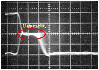
At its most basic level, metastability is what happens within a register when data changes too soon before or after the active clock edge; that is, when setup or hold times are violated. A register in a metastable state is in between valid logic states, and the process of settling to a valid logic state takes longer than normal. It will eventually fall into a stable “1” or “0” state, but there is no way to predict which way it will fall or how long it will take. Think of it as tossing a coin millions of times. There are actually three possibilities: heads, tails, or once in a great while the coin just might stick the landing and end up on its edge, if only for a while. The question is, will that while be longer than a clock cycle? That’s metastability.
When data is transferred between two registers whose clocks are asynchronous, metastability will happen. There is no way to prevent it. All you can do is to minimize its impact by placing the two clocks in different clock domains and using a clock synchronization technique at the crossing point. Hence the name “clock domain crossing”.
Putting two clocks into the same clock domain is a declaration that these two clocks are synchronous to each other, and crossings between them do not need to be synchronized. If the clocks are from the same source, or one is derived from the other, then they are synchronous and can be placed into the same clock domain.
Clocks that are asynchronous to one another should always be placed in different clock domains, and any CDCs between them need to be synchronized. Even two clocks of the same frequency should be placed into different domains if they come from independent sources. Unfortunately, two independent clock sources of the same frequency will drift relative to one another over time and cause metastability problems.
Synchronizers
The simplest synchronization method for a single bit is to have two consecutive registers in the receiving domain. This is known as double-register synchronization. By requiring any metastable state that occurs to pass through two registers, it reduces the chance of metastability from 1/r to 1/r2, which is acceptable for most purposes. Data integrity is maintained only by coincidence. Since it’s only one bit, the only two possibilities are that it will happen to match either the preceding clock cycle or the subsequent clock cycle.
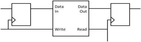
One of the most popular methods of passing data between clock domains is to use a FIFO. A dual port memory is used for the FIFO storage. One port is controlled by the sender, which puts data into the memory as fast as one data word (or one data bit for serial applications) per write clock. The other port is controlled by the receiver, which pulls data out of memory; one data word per read clock.
Two control signals are used to indicate if the FIFO is empty, full, or partially full. Two additional control signals are frequently used to indicate if the FIFO is almost full or almost empty. In theory, placing data into a shared memory with one clock and removing the data from the shared memory with another clock seems like an easy and ideal solution to passing data between clock domains. For the most part it is, however generating accurate full and empty flags can be challenging.
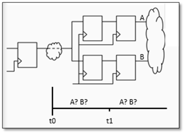
Another CDC issue that must be addresses is that of data reconvergence, when two data signals are combined after being independently synchronized between the same two clock domains. This is a problem because synchronization is inherently an arbitration to avoid metastability. A new value will be correctly clocked, without metastability, on one of two successive receiving clock cycles. There’s no way of knowing which. The two signals in question can be arbitrated differently and can end up being clocked into the receiving domain on different clock cycles when correct operation depends upon their remaining in step. Think again of the coin toss. With a single bit, it’s all but certain that the coin will end up either heads or tails, but with multiple bits, you’d need either all heads or all tails. That’s a losing bet.
The implication is that, for a data bus that crosses clock domains, having individual synchronization on each of the bits will not work reliably. One solution is to generate a single bit “data valid” flag which indicates that the data is stable. Synchronize that flag across domains, and then use it to enable the clocking of the data bus into the new domain.
Another solution is to ensure that the data itself is “gray” (only one bit changing on any given clock cycle) with respect to the receiving clock. This is easier when crossing from a slower to a faster domain because you can be sure there will not be multiple changes from the perspective of the receiving domain. The handshake synchronizers use two m-flip-flop synchronizers to generate request and acknowledge signals.
How to identify CDC Issues:
Blue Pearl Software’s Advanced Clock Environment (ACE) provides a graphical representation summarizing data paths between clocks and can make recommendations for grouping of clocks into clock domains. With ACE, designers can identify clocks to better understand how they interact with synchronizers in the design. This allows users to quickly identify improper synchronizers or clock domain groupings that cause CDC metastability.
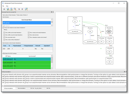
ACE addresses a fundamental chicken-and-egg problem with automated CDC analysis. To perform a CDC analysis, you first must properly define your clock domains, but in order to automatically define clock domains, you need to perform a CDC analysis. ACE does this by performing a quick-and-dirty CDC analysis that recognizes only double-register synchronization, and then by explicitly assuming that two clocks are in the same domain if a high percentage (80% by default) of CDCs are unsynchronized. Then the clock domains, whether defined automatically or by the user, are analyzed and graphically displayed.
The overall goal of ACE is to enable engineers to find metastability issues in designs by properly grouping clocks into clock domains. Design and Verification engineers use ACE to ensure the clock domains are properly specified before running a CDC analysis. ACE will quickly find errors in clock domain groupings or find/recommend appropriate clock domain groupings for a circuit that is synchronized. Only then can a correct and comprehensive CDC analysis be performed.
Next, the Visual Verification Suite’s CDC Analysis understands FPGA vendor clocking schemes, saving enormous resources to set up designs. The CDC analysis has built-in intelligence that helps set up the CDC run and rapidly debug issue found using the built-in cross-probing and schematic display.
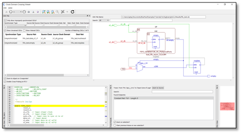
One of the strengths of the Visual Verification Suite’s CDC analysis is that it flags all CDCs, whether unsynchronized, properly synchronized, or improperly synchronized. For example, using a double-register scheme on a single bit is perfectly appropriate, but a multi-bit bus requires a more robust synchronization technique. The user even has the option to find what we call “Clock Equivalent” crossings, which are clock-to-clock interactions within the same clock domain.
Visual Verification Suite, used early and often in the design process as opposed to as an end of design/sign-off only tool, significantly contributes to design security, efficiency, and quality, while minimizing chances of field vulnerabilities and failures.
To learn more about the Visual Verification suite, please request a demonstration.