Thanks to their performance, flexibility and “any-to”outstanding interfacing capabilities, FPGAs are incredibly popular in high reliability applications. They are often used in space systems such as satellites, launchers, aerospace, and autonomous vehicles. In these high reliability applications, depending upon the use case, the system must be able to keep operating or gracefully and safely fail, should an error occur.
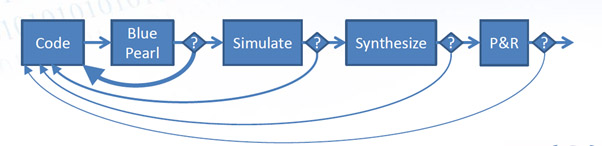
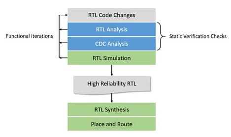
Developing high reliability FPGAs is a complex task which must be considered holistically as part of the wider system. One common step deployed in high reliability flows is the enforcement of RTL development guidelines. These guidelines will contain rules which ensure key elements of the designare setup correctly, such as:
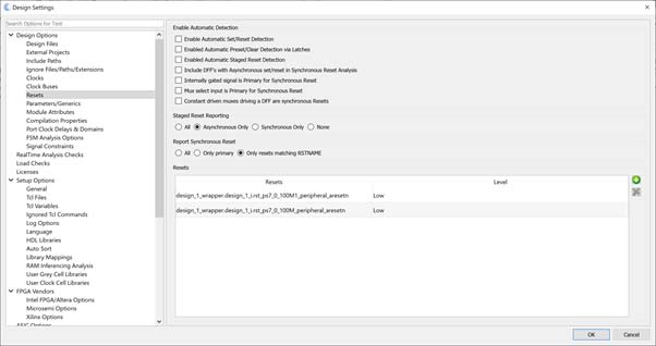
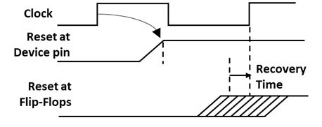
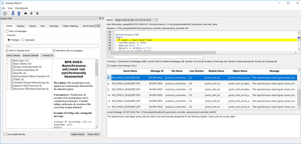
- All flip flops are reset – Relying on the initialised state at power up can lead to unpredictable behaviour which can result in loss of the mission. One example of this was the NASA Wide-Field Infrared Explorer lost due to reliance on the power-on default state
- Vectors are of correct sizes and types – This ensures overflow of incorrect translation does not occur as was the case with Arianne 5 initial launch, in which a 64-bit floating-point number was translated as a 16-bit signed number.
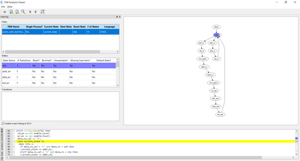
- State machines and counters cannot enter an incorrect state due to a single event effects (SEE)
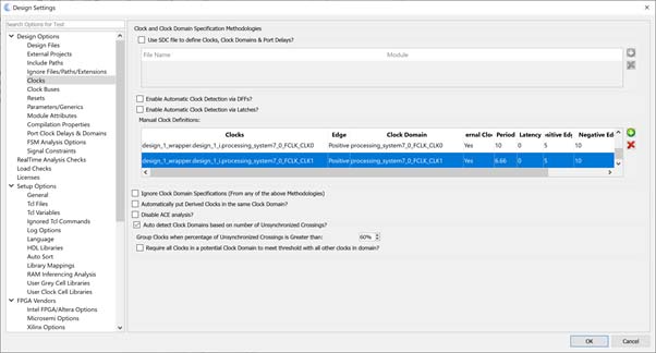
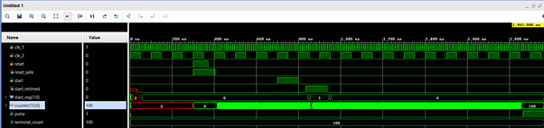
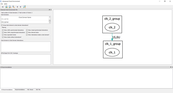
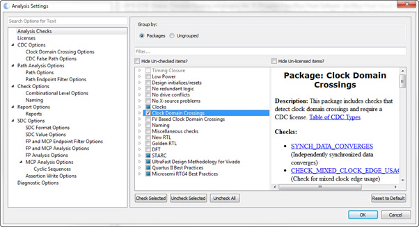
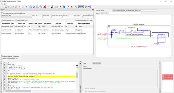
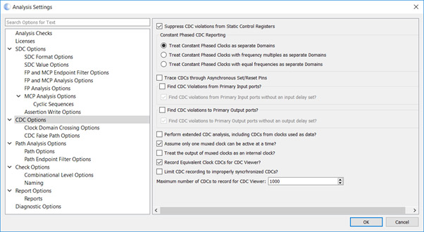
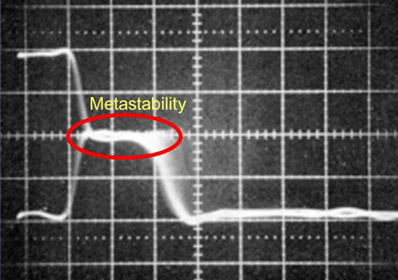
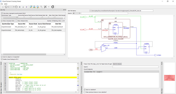
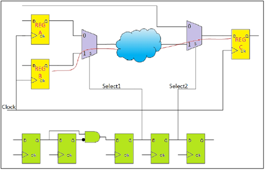
- Clock domain interactions are safe and data crosses without the potential for corruption.
- Naming conventions and coding styles are complied with to ensure readability and portability across projects.
- Coding structures which are likely to cause safety issues are not used. For example, latches, not full defining if statements, gated clocks etc.
- Mismatches between simulation and synthesis interpretations of RTL
EXAMPLE OF BAD CODING:
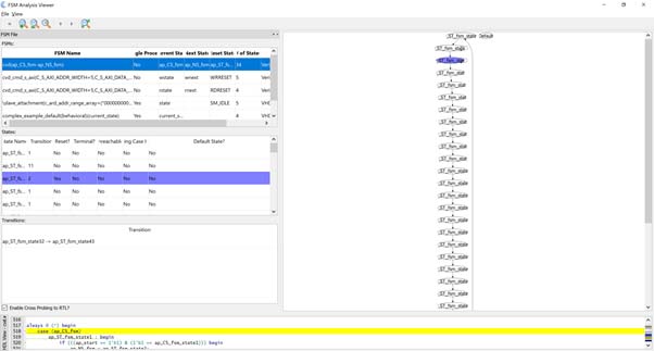
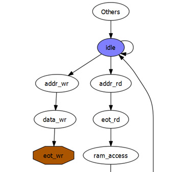
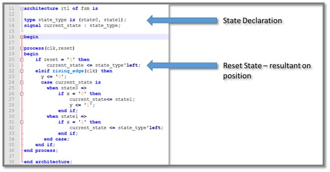
One example of a bad coding structure is demonstrated below in a state machine reset example. While technically correct, the state machine relies upon the position of the state declaration for the reset state. Changes made later to the state machine may result in a change to the behavior. If left as is, this could cause system issues as well.
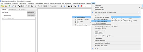
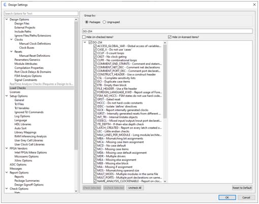
So how would you check for coding issues like this? There several different coding standards which can be used. An example is the D0254 working group, Centre National d’Études Spatiales (CNES) VHDL coding standards.
BUILT IN AND CUSTOM RULE PACKAGES:
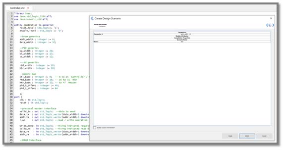
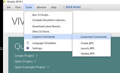
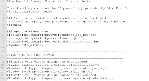
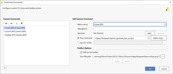
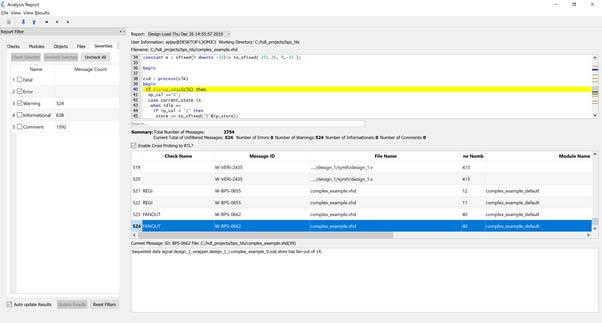
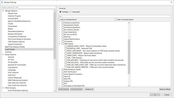
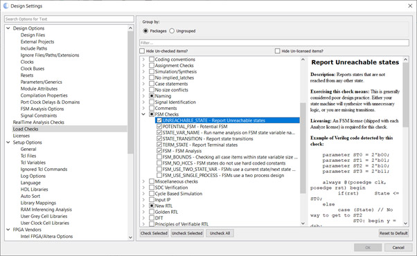
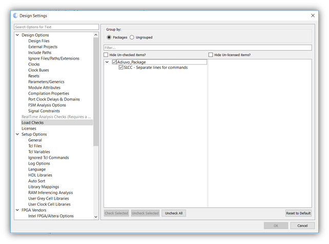
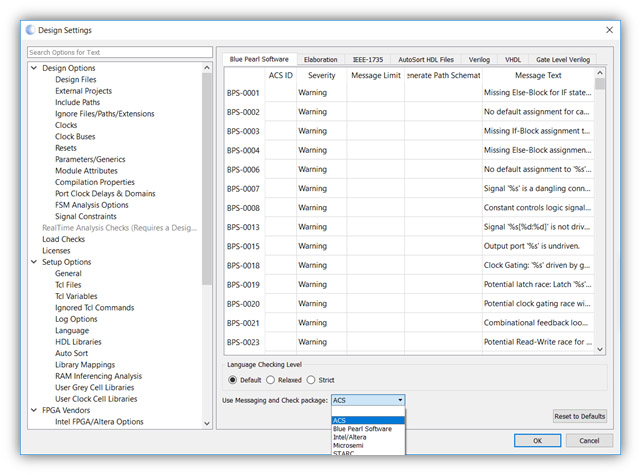
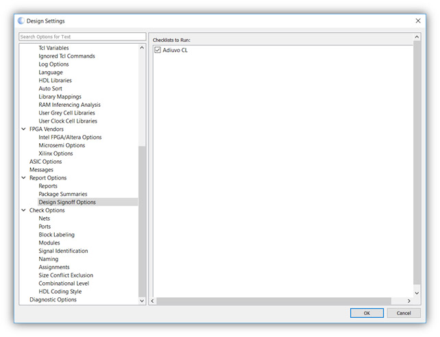
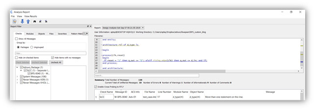
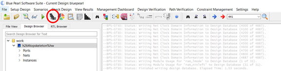
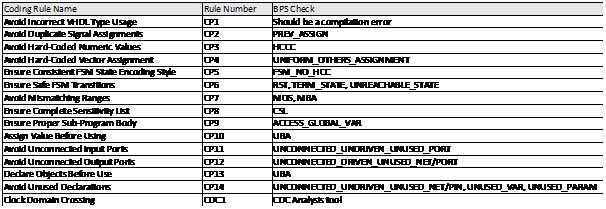
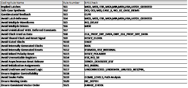
Blue Pearl’s Visual Verification Suite provides several hundred of built in checks which can be used to validate high-reliability guidelines. Some rule checks like the DO-254 coding standards are implemented already within the suite as a package.
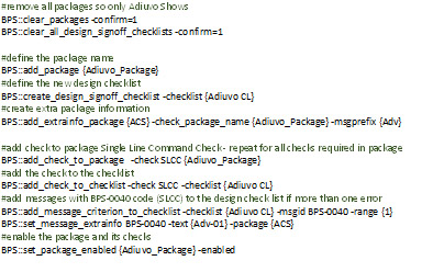
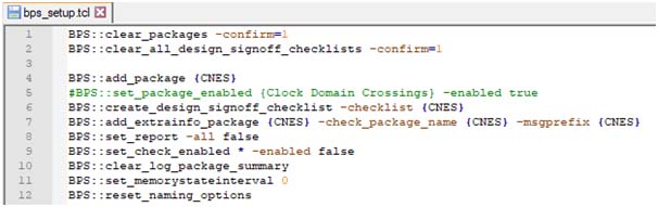
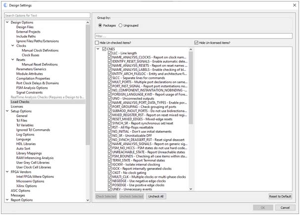
Alternatively, if a different guideline standard is to be used, e.g. CNES, a separate package can be implemented by defining a custom package. This custom package takes the formof a TCL file and can define a custom BSP package.
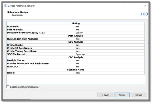
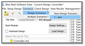
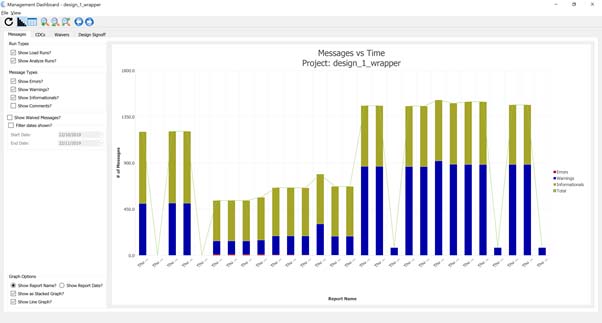
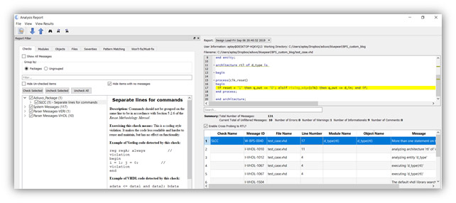
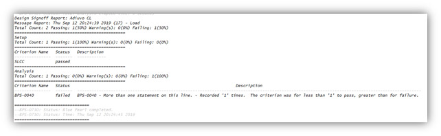
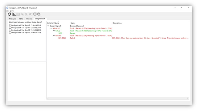
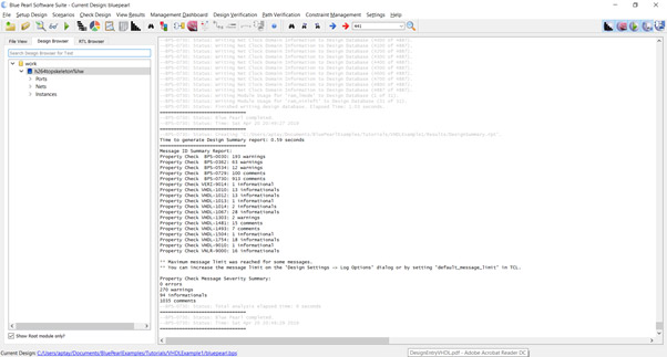
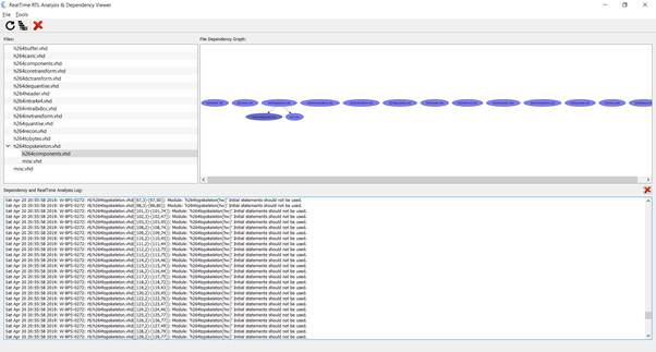
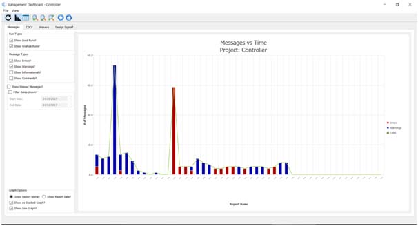
Once the packages are defined, they can be used to check the RTL source files.The maturity of the design can be assessed by tracking the warnings over time. This capability is provided by the suite’s Management Dashboard. Using thedashboard, you can see the number of errors and warnings received as the development progresses. Of course, this should be trending down over time as the issues are addressed.
Using the Management Dashboard in this manner also provides metrics on the impact of requirement changes as the development progresses. In the image below you can see the initial development errors and warnings being corrected before a change of requirements leads to additional increased effort. Metrics such as this are very useful for project management and change impact assessment.
Blue Pearl solutions provide developers of high reliability systemsthe ability to verify and debug their FPGAs prior to implementation, leveraging automated industry standard verification rules and guidelines. Only with such analysis can designersensure the RTL which enters synthesis and simulation is of the highest quality. In addition, the Management Dashboard enables the maturity of the RTL development to be established, providing great metrics on the project for the project management team.