Modern FPGA designs are complex systems. They may include processor cores, RTL code and, increasingly, modules developed using High Level Synthesis (HLS).
Of course, we still want to analyse the custom RTL created and the overall design for compliance with design methodologies e.g. STARC, Reuse Methodology Manual and Xilinx UltraFast Design Methodologies. We may also want to analyse at the design level to ensure all Clock Domain Crossings (CDC) are safe, along with identifying Longest paths and False and Multi Cycle paths which will impact timing constraint creation.
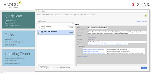
When we are working with Xilinx devices, we can include the Blue Pearl TCL Store Add Ins. These enable us to create new projects, as well as load and update a design from Vivado directly into BPS.
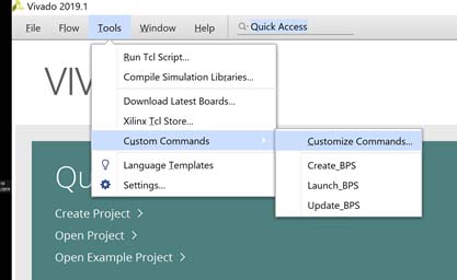
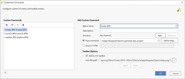
Once the BPS scripts have been installed, we can use the Tools menu to create three new custom commands: Create_BPS, Launch_BPS and Update_BPS.
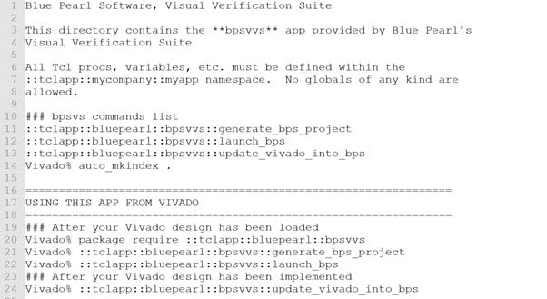
We can find each of the TCL commands to be used for each custom command in the readme file installed with the TCL store add in. On my windows system this was available under the following location.
C:\<user>AppData\Roaming\Xilinx\Vivado\2019.1\XilinxTclStore\tclapp\bluepearl\bpsvvs
You can also find a logo under the same directory that can be used to label the commands.
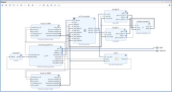
With the TCL store integrated we can then create our design. I used the following to demonstrate a design of sufficient complexity:
- Zynq Processing System Configured for ZedBoard
- HLS Callendar Van Dusen Equation – This design uses floating point representation.
- RTL Implementation of the Callandar Van Dusen Equation – This design uses IEEE VHDL 2008 Fixed Point number representation.
- AXI Interconnect – Connects the HLS and RTL blocks to the processor enabling a SW based solution.
- Processor Reset Blocks
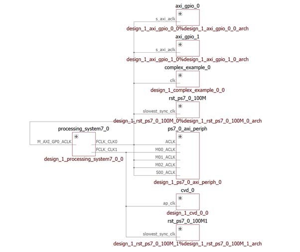
To create a sufficiently complex clocking scheme, the HLS and RTL blocks will be placed on different clock domains (FCLK0 and FCLK1).
The complete design looks as below.
Once the design has been completed in Vivado, we can generate the output products and use the Blue Pearl TCL store commands to create a new project, and then open the project in BPS.
This will contain all of the RTL files used within the design and represent not only the custom developed RTL but also the RTL created IP blocks and the HLS block.
Before we can get the design to successfully load for analysis, we need to make some changes to the design settings. This includes:
- Setting the VHDL Language 2008 – this is due to the use of the fixed-point libraries in the RTL module
- Set the Xilinx Libraries to the correct version – In this example I used Vivado 2019.1
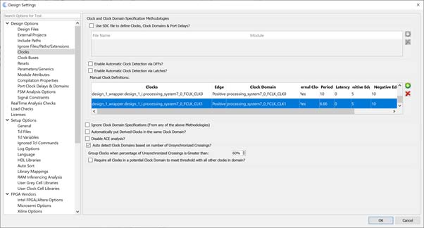
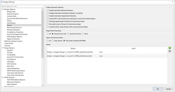
I also defined the Clocks and the Reset from the Processing block. These are defined in the Design Settings -> Clocks and Design Settings -> Reset tab
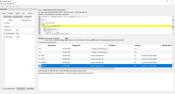
With these changes we can then successfully load in the design to BPS and start analysing and filtering the load messages.
By opening the results view and looking through the detailed messages, we can then assign waivers to the messages raised. These waivers indicate if the message needs to be addressed (Must Fix) or does not need to be fixed (Won’t Fix).
When we are working with large groups of messages, we can use regular expressions to waive several messages to either must or won’t fix at once, easing the analysis.
Once this analysis is completed, we will have several issues remaining in the design which are flagged as Must Fix.
We can also observe the design in the schematic viewer to ensure the design architecture looks like the block diagram in Vivado.
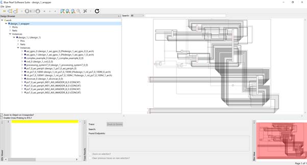
Within the schematic view we can double check to see that all the instances included in the Vivado design are visible.
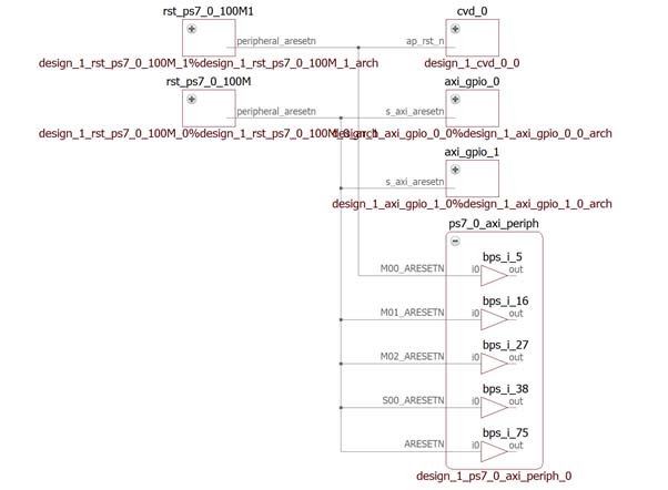
We can also configure the schematic viewer to observe the clock and reset trees within the design using the Clock Tree Schematic and Reset Tree Schematic views.
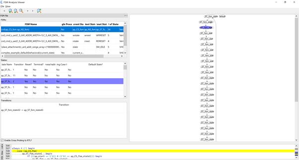
With the design loaded we are then free to explore the FSM viewer to analyse any issues raised in the load analysis.
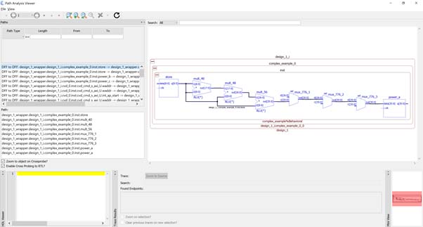
All this information is available as soon as the design loads. We can also then run design analysis to identify any issues such as clock domain crossing, path analysis and false / multicycle paths.
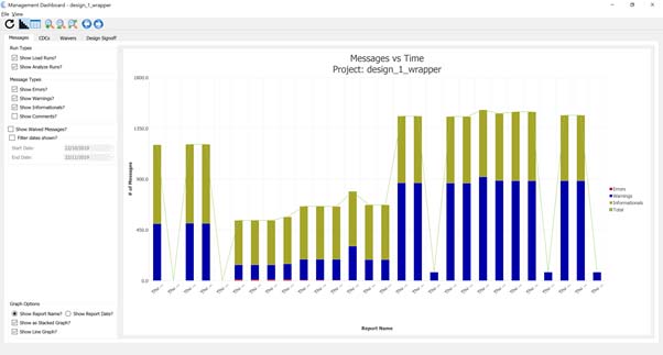
Finally, you can observe the maturity of the design as it passes through the load and analysis phases using management dashboard. This enables us to see the number of open issues and therefore the project maturity we progress through the design cycle.
Wrapping up, we can see that we have been able to load in a complex design which consists of different elements e.g. processing system, HLS IP and Standard Xilinx IP into Blue Pearl Software and this enables us to check for design level issues.
You can find the example Blue Pearl and Vivado projects here.